
What's inside Microsoft's Maia 200 AI Chip
A look at the new AI Accelerator ASIC from Microsoft.

It is becoming clearer than ever that training of Large Language Models (LLMs) is no longer the real bottleneck in today’s age of AI. Instead, it is inference — the usage of AI, particularly in light of agentic systems, exceeds compute and memory and power requirements far more than training does. Today’s models, and the available hardware architectures that run them, can perform prefill fast, but suffer on decode. When you look deeply, you realize that compute is no longer the bottleneck — it’s where memory and storage are, and the cost of moving data between memory/caches/storage and compute. The closer you bring memory to compute, the faster inference becomes. However, the cost, as well as technical complexity, of bringing memory closer to compute is still a challenge. Every leading hardware company in the AI market is trying to solve it in different ways. I have talked about how Nvidia, Cerebras and Groq are trying to approach this in previous posts.
What’s also becoming clearer is that hyperscalers, as well as leading AI labs, are now putting a lot of focus on building their own Application Specific Integrated Chips (ASICs). There are multiple reasons why, but some in particular that weigh more than others are:
GPUs are general purpose and not designed for AI workloads.
Reducing interconnect bottlenecks on chips and architectures brings about incredible performance gains and cost optimizations.
Bringing memory closer to compute and increasing its capacity pays dividends.
This is why Cerebras has their AI specific ASIC. That is why Google has their TPUs, and Groq their LPUs. That is also why Amazon is working on an in-house ASIC accelerator (chip). And that is why, coming to the topic of this post, Microsoft has released their custom AI centered ASIC accelerator, called Maia 200.
As I normally do, I will not go into exhaustive details of the architecture of Maia 200 but will focus on parts of its architecture that Microsoft claims make Maia 200 a low-cost, low-latency, performant inference accelerator, and why that may be the case. Microsoft calls it the Hyperscaler Inference ASIC.
Note: The term ‘accelerator’ is used interchangeably to mean the main chip. The acronym used these days is: xPU (for GPU, LPU, TPU, etc).
Compute and Memory
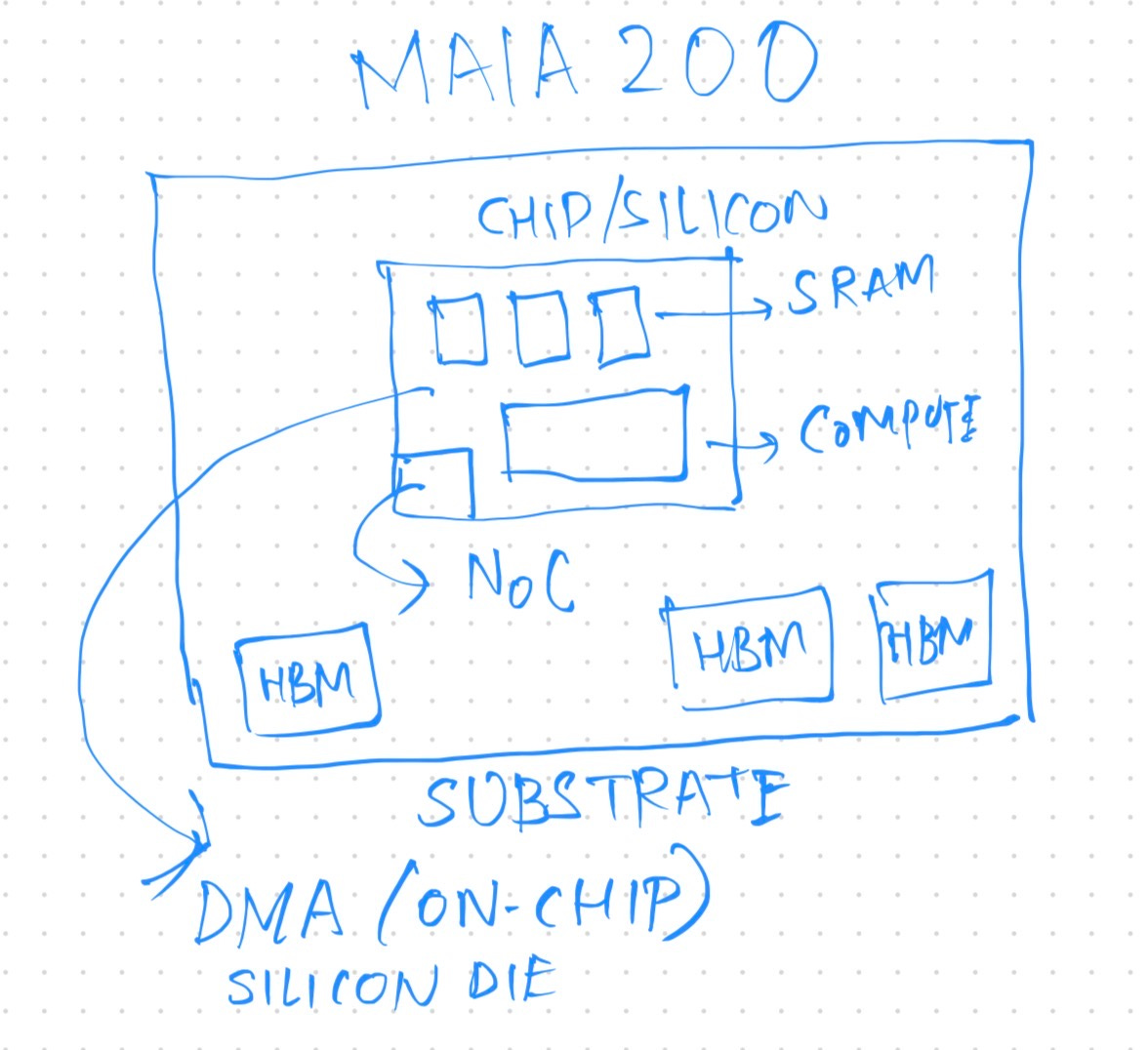
Maia 200 at its core uses a micro-architecture (for both compute and memory) built on top of TSMC’s latest N3 process. The smallest unit of that architecture is called a Tile — it groups together a block of compute as well as local storage (SRAM). The local storage/memory available to a Tile is called Tile SRAM (TSRAM) and is the fastest, lowest-latency memory available to compute on the chip (on the same die/silicon as the compute).
Tiles and Clusters
Multiple Tiles are grouped together in Clusters. Each Cluster has access to cluster level local storage, which is called Cluster SRAM (CSRAM).
The single Maia 200 chip contains 272MB of SRAM capacity. In order to match the hierarchy of compute, SRAM is divided into TSAM and CSRAM, as described above. Outside the chip, but on the package (substrate) on which the chip/die is found, there are HBM3e modules available, totaling to about 216GB of HBM memory.
Note: The package is also known as the substrate to distinguish it from on-chip elements which are found on the piece of silicon where the chip is.
Direct Memory Access sub-system
In order to take advantage of this multi-tiered hierarchy of compute and memory, a multi-level Direct Memory Access subsystem exists on-chip as a hardware unit. This resembles the DPU found in the Nvidia Vera Rubin platform. Each Tile has access to Tile-level DMA, and each Cluster has access to a cluster-level DMA. The goal of the DMA is to ensure seamless data movement across components without stalling compute, introducing latencies, and maximizing hardware level synchronization requirements. The Tile DMA subsystem allows easy movement of data between compute, Tile SRAM, and Cluster SRAM. The Cluster DMA subsystem allows easy movement of data between Tile SRAM and HBM modules found on the package. Each Cluster has a dedicated core responsible for controlling and synchronizing the movement and execution of data across several Tiles. You can think of these as Tile-level scratchpads and Cluster-level scratchpads, where compute does not need to wait for data to be pulled from the on-package HBM (where the model weights are stored, for example). The different levels in the hierarchy take care of movement of data independently across different layers so that compute is not waiting on data — which is the primary bottleneck with GPUs.
Support for narrow precision data types
Another advancement in the Maia 200 architecture is its support for narrow precision data types, also know as bit-wise floating point operations. Traditionally, the larger the size of data type, the more information (and nuance) can be handled by layers of neural network. At the same time, computation as well as storage costs go up because hardware has to store and move more data as well as perform more complex computations. Hardware companies and AI labs are increasingly learning that if they use narrow precision data types like FP4 and FP8 (and if they mix different data types together), they can almost solve the problem of loss of accuracy (resulting from a smaller data type) and high cost (resulting from a bigger data type). Maia 200 has been designed from the ground-up to support these narrow precision data types. The Tile compute can perform computations in FP8, FP6, and even FP4. It can also support mixed precision computations, such as between FP8 and FP4. For inference, this results in incredible gains in tokens/second performance, as well as reductions in tokens/watt power usage.
Network
All of these advancements in the architecture don’t mean anything if there’s no fast, low-latency network interconnect available to support the movement of data. Maia 200 has two dedicated on-chip NICs.
Network on Chip (NoC)
External NIC
Both of them are built on the same die as the compute chip. They provide fast bi-directional (2.8 TB/s) bandwidth to support fast movement of data, both internally across on-chip components and on-package components, and across the scale up fabric when multiple Maia 200s are connected together (as we will explore later). This integrated NIC becomes a core element for the multi-level DMA sub-system, as it allows for movement of data between Tiles, TSRAM, CSRAM, DMA engines, HBM controllers, etc.
With Maia 200, Microsoft has paired the on-die NIC with their AI Transport Layer (ATL) protocol which enables advanced networking features such as unicast, multicast, packet spraying, multi-path routing, congestion control, and resiliency. With an optimized communications protocol layer, having NICs on the die result in low power and cost overhead, which is inherent in external, off-chip NIC interfaces.
Scale-up fabric
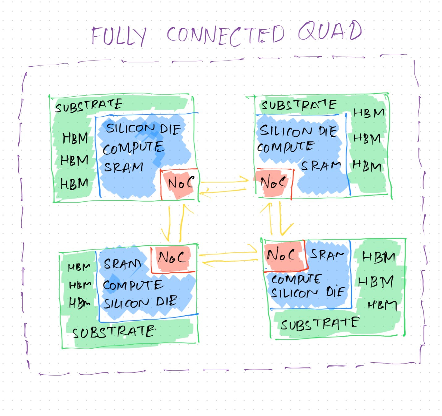
A group of four (4) Maia 200 chips can be connected together to form a Fully Connected Quad (FCQ). These are four Maia accelerators working locally in tandem. No external switch or ethernet is needed for communication. Each of them is directly connected to the Network on Chip (NoC) on each Maia 200 die. This forms the first tier of Microsoft’s 2-tier topology for Maia 200 network scale. These FCQs are fast, have a lot of compute and storage/memory available, and are equipped with an on-die fast ethernet which ultimately results in optimized parallel computations at low cost and low latency.
In the second tier, multiple FCQ groups can be connected together using commodity ethernet switches to provide up to 6144 Maia 200 accelerators. With ATL and integrated NIC, communication across FCQ groups can be tightly coupled both within the rack and across the rack.
Another advantage of using a 2-tier network topology is to keep high intensity inference traffic inside the FCQ as much as possible. This includes traffic like KV updates, parallel tensor computations and others. The second tier then takes care of everything else, leaving the first tier unburdened by baggage.
Conclusion
This provides a highly performant but reliable scale up fabric for inference that is designed to co-exist with other hardware in Microsoft’s Azure racks and data centers. It’s a GPU-class accelerator that is done Microsoft’s way, built for running large SOTA reasoning models.
Once more we see a custom silicon architecture focused on solving the memory and interconnect bottlenecks in unique ways.
Custom silicon ASICs are no longer an afterthought. Hyperscalers now understand the bottleneck better than before. They also understand that a custom-silicon, in-house ASIC is the way to achieve both margins with performance and cost, as well as build a hardware moat.
Thank you for reading!
References