
What's inside the world's fastest AI processor: Cerebras Wafer Scale Engine
A look at how Cerebras has achieved a fast AI training and inference chip.

On the heels of my posts about LPUs and Nvidia’s Vera Rubin platform, I sat down last week to understand what Cerebras.AI is and why they claim to have built the fastest infrastructure for AI training and inference. This, once again, will be my simple attempt at explaining the Cerebras architecture as best as I can.
The Problem We Are Trying To Solve For
GPUs are great at compute, particularly parallel compute. Many GPUs can be clustered together to increase parallelism. However, that does not necessarily improve the performance of the entire system. AI workloads—both training and inference—are not only compute-bound, but also memory-bound. The compute problem is being solved by improving GPUs and adding many of them together to work in clusters. But memory is still a big problem that every AI hardware provider is struggling with.
A neural network’s computations can happen on a series of GPU cores in parallel, but the model’s weight cannot be stored inside GPUs. In order for computations to be meaningful, model weights—the model’s knowledge—have to be moved back and forth all the time. This is expensive: it requires energy, and is prone to I/O latency (among other complexities). On top of that, a given state-of-the-art (SOTA) model today has billions of weights (parameters) if not trillions. The closer those weights are to compute, the faster the computation can happen. The closer they are, the less energy is needed to move weights back and forth. That, in and of itself, ultimately is the big problem with AI infrastructure today.
Latest GPUs have very, very limited on-chip SRAM (which is the fastest and closet to the cores). This is likely in MBs. Therefore, in order to train and run large SOTA models, the weights have to be stored in high bandwidth memory (HBM) modules, such as DRAM. The problem is: HBM is not close to GPU cores. In order for a model’s computation to run effectively, a lot of weights have to be moved back and forth between the HBM and the cores (and everything else that exists in between, which we call the fabric). The throughput of HBMs—what is known as memory bandwidth—is limited, and so is the interconnect throughput—which is known as interconnect bandwidth. Adding more GPUs to the infrastructure simply moves the bottleneck: the memory.
We discussed how Groq’s LPUs have tried to solve this. In this article, I will explain how the Cerebras system is trying to solve the same problem.
The Semiconductor Yield Challenge
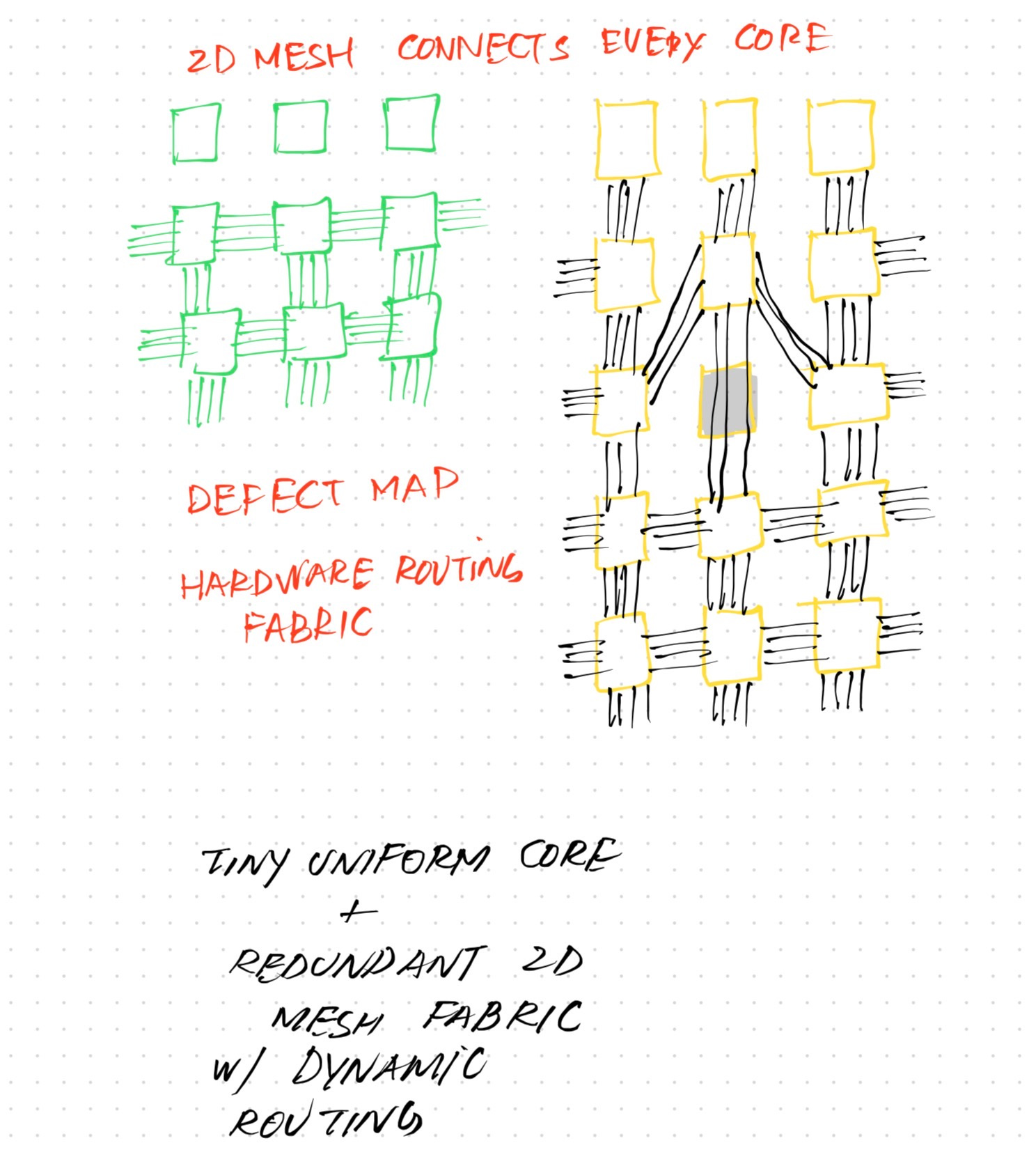
Chips have traditionally been made out of dies, which are cut out of silicon wafers. Since silicon wafers can have impurities and other constraints which can leave parts of the wafer unusable, the traditional approach to ensuring the most number of functional dies are extracted from a wafer of silicon is to cut the wafer into many smaller dies. This is called the yield—what percentage of dies from a wafer are functional. If the size of the die is large, the yield goes down. Thus, cutting them into smaller-sized dies has always made sense. The down-side though is that you cannot pack many chips in the same silicon. This requires a distributed architecture where a wafer is broken up, and then combined back again using different techniques to distribute compute, processing, instructions and memory.
Cerebras took a different approach. They thought that since defects in wafers are inevitable, they should instead design their architecture for defects. What this means simply is that they take a very large piece of silicon wafer and put many chips on top of the dies inside the wafer, and provide a 2-D mesh that connects each chip/die to every other chip through redundant pins and paths. This means that when the entire wafer goes into production, they can figure out which dies are non-functional, and automatically route traffic and data around them. All of this at the hardware level!
Wafer Scale Engine
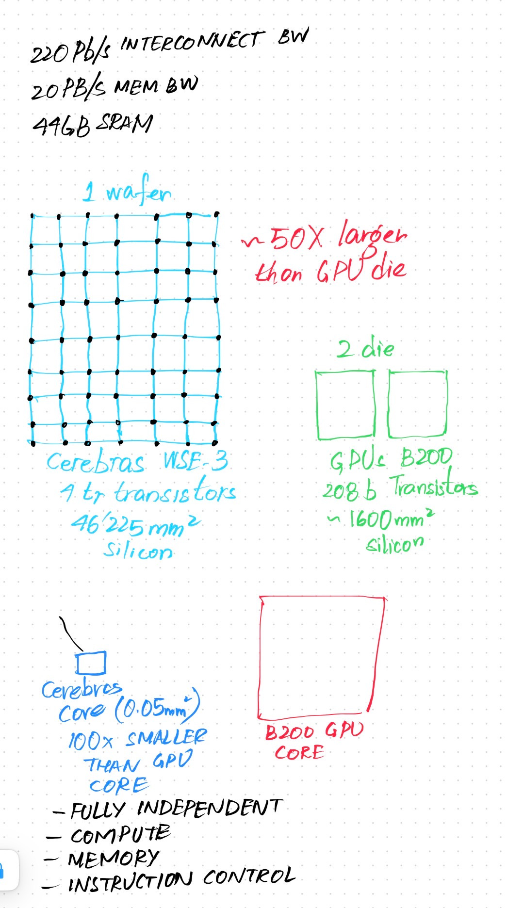
They call it the Wafer Scale Engine. One giant processor, on a single silicon wafer, that measures 46’225 square meters. This houses 84 dies, and each die carries 10.7k cores on it. By keeping the size of the core tiny, they are able to pack around 970k cores inside the wafer, out of which 900k cores are active and functional. That is roughly 7% of the wafer that’s impure and defected—but by packing the wafer dense and adding redundancy, the yield was increased incredibly.
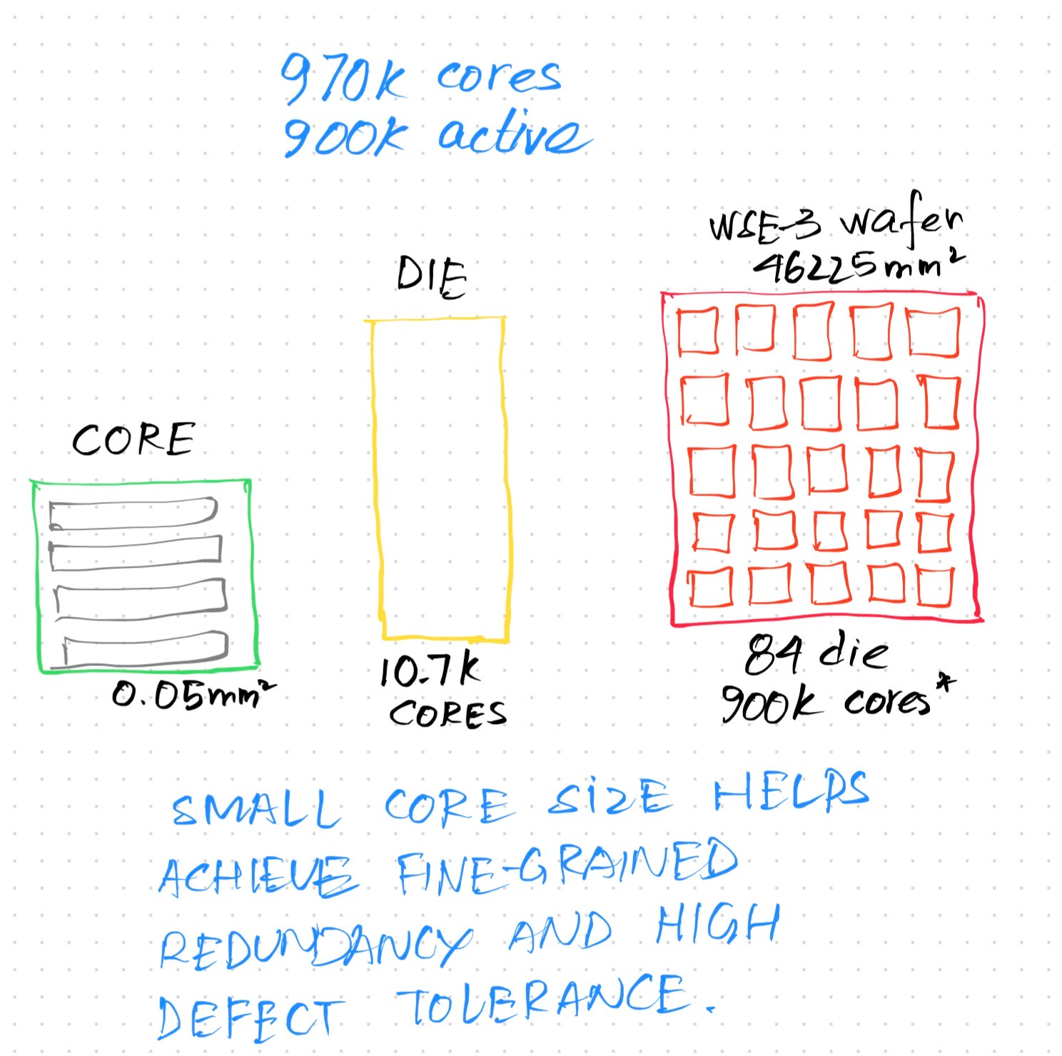
Each tiny core is independent and carries within it its own independent compute, memory and instruction control.
Compared to a standard GB200 Nvidia GPU, this single wafer offers 44 GBs of high speed SRAM on-chip memory (right on the silicon wafer), 20 PB/s of memory bandwidth between the core(s) and SRAM, and 220 Pb/s of interconnect bandwidth across the entire wafer. This single wafer is almost fifty times larger than a B200 GPU die, and packs a massive array of 4-trillion transistors on it compared to billions on B200.
With fine-grained redundancy (routing around defective chips), ultra-dense compute (many tiny independent chips on a single big piece of silicon), and self-healing routing fabric, they are able to make every wafer a high yield, fully functioning processor with high speed on-chip memory available.
This single wafer based processor removes the following long-standing barriers to optimized AI compute design:
Inter-chip communication: many GPUs working together require a lot of back and forth communication via data paths that is not only costly but introduce delays.
Memory fragmentation: not having access to a large amount of on-chip memory means that memory has to be distributed across the infrastructure in the form of separate HBM layers, and then moved back and forth for computation.
Distributed orchestration: with multiple GPUs and HBMs scattered around, the system has to ensure proper, timely orchestration in order for neural network computations to execute. The more layers there are in the infrastructure, the more prone it becomes to latency and complexity.
The Wafer Scale Engine (WSE) is a processor on a single silicon with access to a large amount of on-chip SRAM and high interconnect bandwidth to optimize the back and forth moving of data along data paths. The redundant design of the wafer architecture makes it possible for Cerebras to pack a lot of cores on a single, big wafer, utilizing more of the wafer by smartly routing, at the hardware level, around defective dies.
Larger chips don’t yield. Defects are inevitable — why not design for them.
The Cerebras System
The Wafer Scale Engine is the core of Cerebras. Of course, you can’t do anything with the hardware alone. You need an entire system and supporting software around it. This is where the Cerebras System (CS) comes in. Obviously, this system includes the entire rack, the power supply unit, the liquid cooling system, and everything else in between that makes all of this possible. These are naturally custom designed to meet the needs of the high powered processor. I won’t go into those in this article because they aren’t uniquely interesting.
This also encompasses the Cerebras Software layer, which enjoys compatibility with existing tooling such as PyTorch and TensorFlow. It includes the Cerebras Graph Compiler which extracts deep neural networks out of existing tools, and generates an executable that can be run efficiently on WSE. There is a lot more to that as well as the development tooling and API, but I won’t go into that in this article.
However, I will talk about the proprietary sparsity-harvesting technology they use for their cores.
Sparse Linear Algebra Compute (SLAC) Cores
Most of neural network computations are tensor multiplications, which are multi-dimensional matrices being multiplied together and/or with vectors. Most GPU and Machine Learning operations are dense, which means that tensors are packed with non-zero values. However, these tensors can also be sparse: containing 0s. Algebraic operations against 0s are a waste of time, memory and resources. They don’t produce anything. Since GPUs are dense execution engines, even if there are 0s in matrices, they will continue to perform algebraic operations with 0s. This wastes resources. Because GPUs are optimized for dense operations, they can’t smartly skip multiplications (or other operations) with 0s.
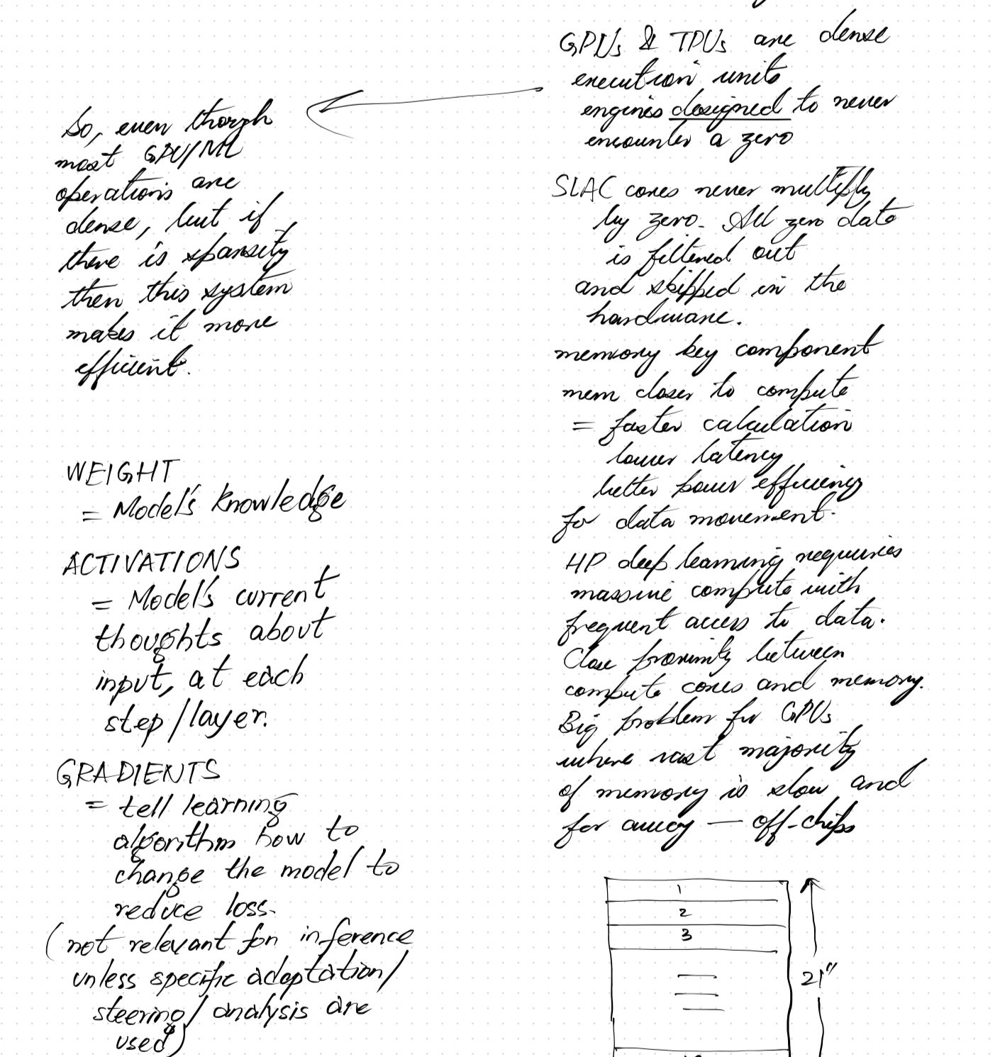
The cores on Cerebras are designed for sparse linear algebra compute. What this means is that the basic building blocks (primitives or kernels) for doing sparse linear algebra, such as matrix multiply (MATMUL), are sparsity aware: if they encounter 0s in the tensors, they will skip those operations. Because these cores are optimized for neural network compute primitives, the result is that the Cerebras WSE achieves industry-best utilization of cores.
Conclusion
With a wafer-scale dense processor, acess to high-speed, low-latency on-chip memory, sparsity aware cores, and the entire system and tooling for compatibility, the Cerebas System offers an interesting solution to problems afflicting AI workloads today.
As we saw with LPUs, moving high-speed, low-latency access to memory closer to compute removes the major bottleneck that leading AI infrastructure companies are trying to figure out. Cerebras, with their WSE, tackle this problem in a uniquely different way.
I hope this deep dive into the architecture was helpful. Thank you for reading.
References
Cerebras Systems: Achieving Industry Best AI Performance Through A Systems Approach